There are different requirements for different project teams and tasks in the system-on-chip (SoC) development process: hardware design, simulation, formal verification, firmware coding, system-level validation, etc. The focus is not so much on individual products, but how they work together to automate multiple phases of the process against executable specifications.
The relatively new IDS NextGen (IDS-NG™) solution, provides a common front end and “dashboard” for all users across teams.
The relatively new IDS NextGen (IDS-NG™) solution, provides a common front end and “dashboard” for all users across teams. Agnisys outlined some of the issues facing chip designers today and several ways Agnisys’ solution can help automate specifications. These challenges include:
- Design of large, complex sets of control and status registers
- Properly handling clock domain crossings
- Obtaining robust but flexible IP for standards-based blocks
- Supporting complex bus protocols
- Interconnecting IPs and custom blocks
- Satisfying functional safety and security requirements

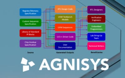
Agnisys generates the complete RTL design for the specified registers and relieves the design team from all the coding work involved. Agnisys make the designers popular with other teams on the project because you also generate Universal Verification Methodology (UVM) models for the verification engineers, C/C++ headers for the embedded programmers, and documentation for the technical writers. This eliminates bugs related to different interpretations of the specification or to using different versions of the specification. Any change to the specification will result in regeneration for all teams so that they remain at the same level.
Agnisys also generates the RTL code necessary to avoid metastability and other clock domain crossing problems (CDCs). When creating the registers, IDS-NG detects if they are in a different clock domain than the system bus or if they are in a unique clock domain that is different from the system bus and the rest of the hardware design. Agnisys supports several well-proven types of synchronization across the CDC boundary, including two-level flip-flops, multiplexors, and handshakes. The software also supports the verification team by generating the relevant assertions for the formal CDC analysis.
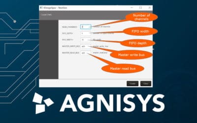
The last blog post discussed the challenges of standards-based IP and introduced the SLIP-G™ library of IP generators. Developers have many options to configure and customize the IP blocks generated by Agnisys. The currently supported standards include General Purpose Input/Output (GPIO), I2C, Timer, Programmable Interrupt Controller (PIC), Direct Memory Access (DMA), Serial Peripheral Interface (SPI), Pulse Width Modulation (PWM), and Advanced Encryption Standard (AES). In all cases, the RTL design, UVM models, programming sequences, and documentation are created.
A typical SoC has many thousands of blocks, some standards-based IP, some licensed from other sources, and some custom designed. Assembling all these blocks into the top-level chip is a big and rather tedious task. Luckily, IDS-NG also automates this process for you. As you would expect, Agnisys generate all the RTL code required to connect the blocks from SLIP-G. You can also specify how custom blocks should be integrated and generate this part of the RTL design as well. Finally, RTL aggregators, bridges and multiplexers for standard buses are generated as needed.

A high quality standard for standards-based IP
The Standard Library of IP Generators (SLIP-G™) has proven to be very popular with users, and this is not surprising. Reuse plays a significant role in system-on-chip (SoC) development.
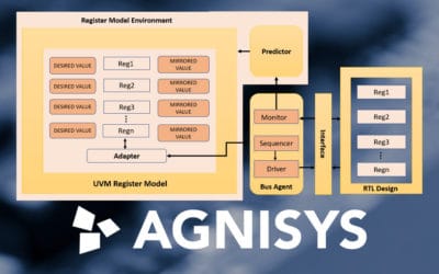
Automating the UVM Register Abstraction Layer (RAL)
This post focuses on the UVM Register Abstraction Layer (RAL), sometimes called the UVM Register Layer. Today’s large system-on-chip (SoC) designs contain many control and status registers, often accessible from embedded software or drivers as well as hardware.
Automation of IP and SoC development
Agnisys has expanded its original focus on register automation to encompass specification-driven design, verification, embedded programming, validation, and documentation of IPs and SoCs This expansion is a testament to Agnisys growth and the many challenges semiconductor development teams face.
Webinar on Embedded System Development Using Agnisys
Embedded System Development Using Agnisys This provides a path that avoids many pitfalls present in a typical flow, such as a slow process, duplicate efforts, wasteful resources, and so on.
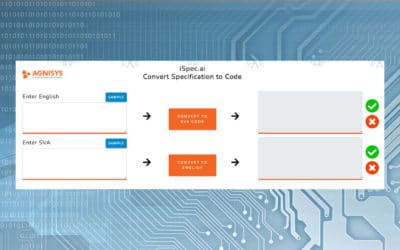
Automatically translate English description into SystemVerilog Assertions
Agnisys has developed a unique approach that uses artificial intelligence (AI) and machine learning (ML) to translate English descriptions of design intent into SystemVerilog Assertions (SVA).


