HES™ is a feature-rich family of SoC/ASIC pre-silicon physical prototyping and hardware emulation boards. The family features boards with high-performance devices from either Xilinx (including Virtex-7, Virtex UltraScale, Virtex UltraScale+ and Zynq UltraScale+) or Microchip (PolarFire and SmartFusion2).
HES high-speed backplanes means boards can be interconnected and designs targeting ASICs or SoCs of several 100m ASIC gates can be easily accommodated. In addition, all boards can be used with Aldec’s range of FMC daughter cards, the widest range in the EDA industry.
HES boards can also be used for algorithm acceleration in High-Performance Computing (HPC) applications, such as High-Frequency Trading (HFT), computer vision and genome alignment.
Xilinx VIRTEX ULTRASCALE+ FPGA Boards
HES-VU19PD-ZU7EV
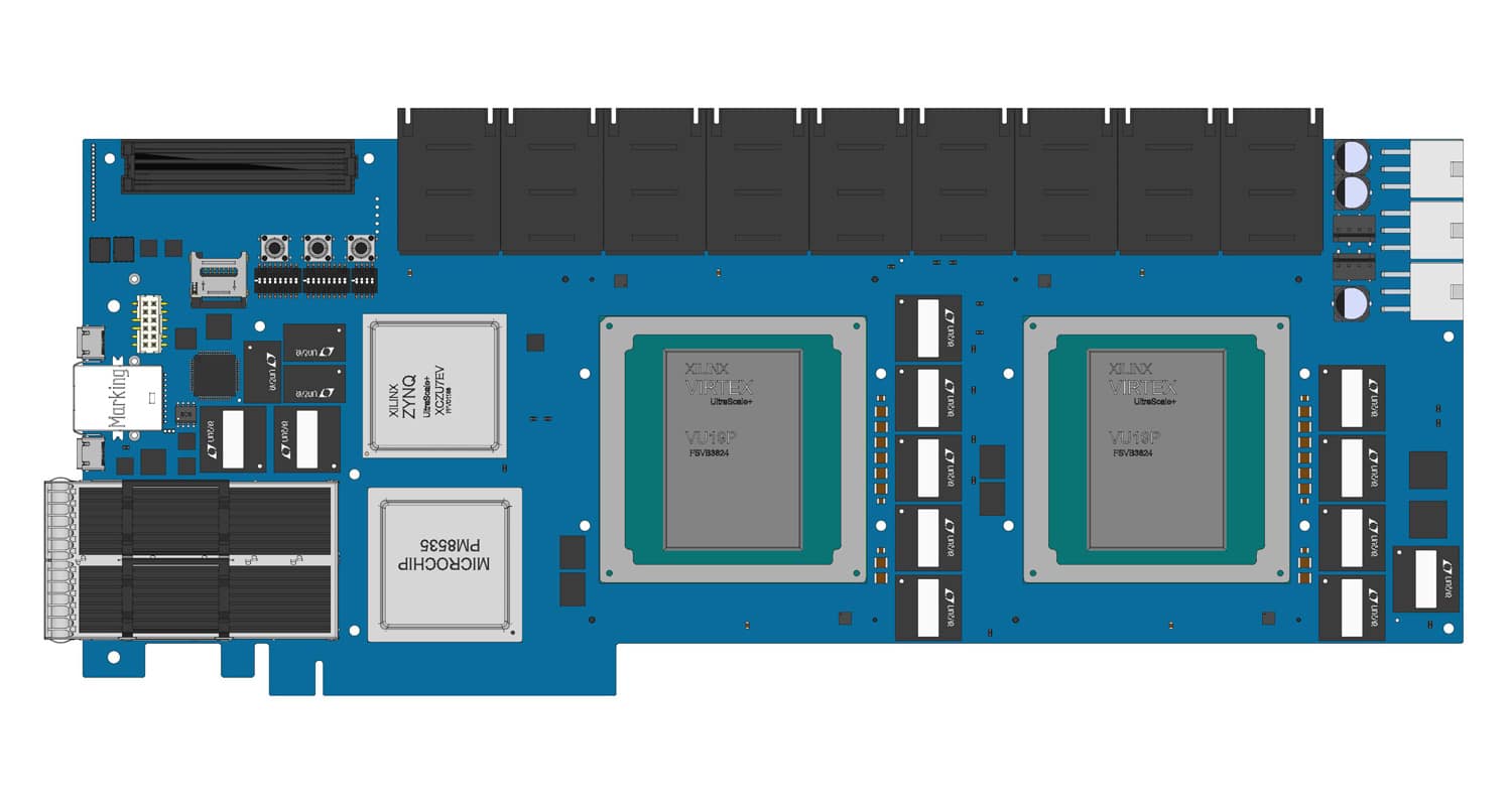
The HES-VU19PD-ZU7EV offers a unique combination of two Virtex UltraScale+ VU19P FPGAs as logic module and one Xilinx Zynq UltraScale+ ZU7EV MPSoC as the host module that features a Quad-core ARM® Cortex-A53, Dual-core ARM® Cortex-R5 real-time processing units, an ARM® Mali-400 MP2 GPU, integrated H.264/H.265 video codec, and UltraScale+™ programmable logic in a 16nm FinFET node This board is targeted for high-speed physical prototyping and emulation of medium to large ASIC designs. The HES-VU19PD-ZU7EV provides 83M ASIC gates and it goes up to 316M gates on a backplane.
There are 5x SODIMM external memory available on the board, 4x are connected to VU19P devices and 1x connected to the ZU7EV device On chip memory for the VU19P device is 166Mb and 11Mb for the ZU7EV device.
HES-XCVU9P-QDR
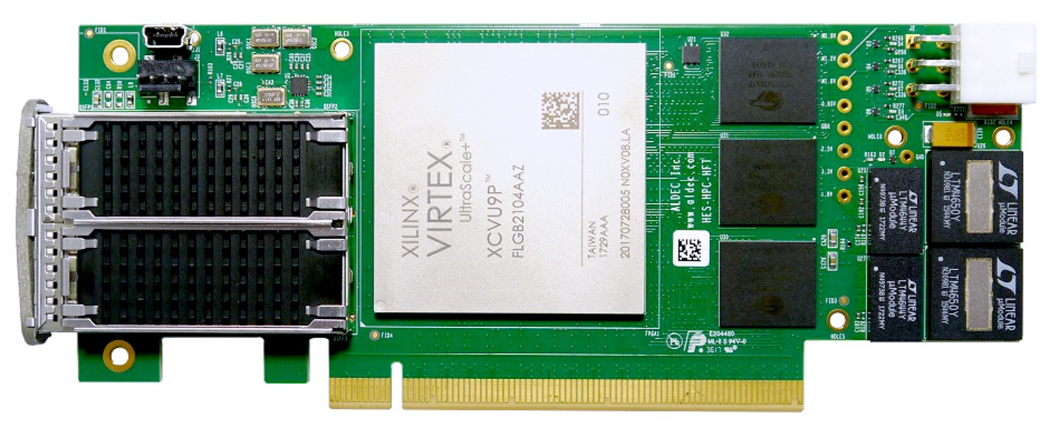
The HES-XCVU9P-QDR board with Xilinx Virtex UltraScale+ XCVU9P FPGA enables High-Performance Computing (HPC) solutions with a need for high-bandwidth and low-latency communication through QSFP28. The customizable FPGA combined with QDR-II+ or DDR4 memory modules provides high throughput for software acceleration, data processing, telecommunications, and more. The PCIe x16 half-length low-profile board easily fits into enterprise rack systems for maximum performance density.
HES-XCVU9P-ZU7EV
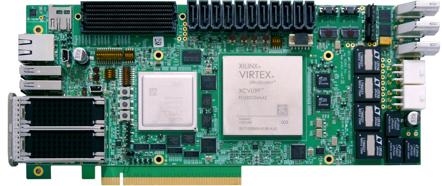
The HES-XCVU9P-ZU7EV is designed for High-Performance Computing (HPC) applications that require immense digital signal processing. The board features a unique integration of a ZU7EV Zynq® UltraScale+™ MPSoC and a VU9P Virtex® UltraScale+™ FPGA. This heterogeneous computing platform leverages a Quad-core ARM® Cortex-A53, Dual-core ARM® Cortex-R5 real-time processing units, an ARM® Mali-400 MP2 GPU, integrated H.264/H.265 video codec, and UltraScale+™ programmable logic in a 16nm FinFET node.
Available onboard external memory resources include three (3) DDR4 SODIMM slots and two (2) modules of 576Mb RLDRAM-3 (1Gb total). On-chip memory for the Zynq® programmable logic includes 11Mb of Block RAM and 27Mb of UltraRAM. On-chip memory for the VU9P programmable logic includes 75.9Mb of Block RAM and 270Mb of UltraRAM.
Xilinx VIRTEX ULTRASCALE FPGA Boards
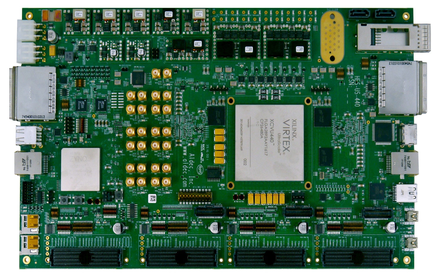
HES-US-440 Prototyping, Emulation and HPC Main Board
The board HES-US-440 offers a unique combination of Xilinx Virtex UltraScale XCVU440 logic module and Xilinx Zynq-7000 host module featuring ARM dual-core Cortex-A9 CPU that allows building a self-contained, one-board testbench for the design. It has been optimized for high-speed physical prototyping and emulation of medium size ASIC up to 26 Million gates or the largest FPGA designs. The board contains two independent SO-DIMM slots connected to UltraScale that deliver up to 64 GB of DDR4 and two RLDRAM3 modules with SRAM-like interface, low latency and aggregated capacity of 1152 Mb. Such a memory-reach board design makes it applicable for numerous High Performance Computing (HPC) applications apart from physical prototyping. It can be also reused for HES emulation applications like simulation acceleration or co-emulation with virtual models.
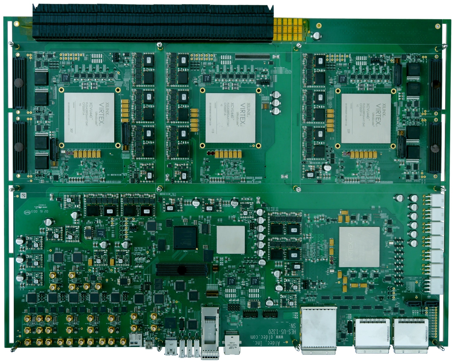
HES-US-1320
Aldec’s large capacity board with three XCVU440 logic modules is targeted to high-speed physical prototyping and emulation of ASIC and SoC designs. The board provides an estimated capacity of 79 Million gates and is easily extendable via backplane and daughter card non-proprietary connectors (BPX & FMC). Each UltraScale FPGA module is connected with DDR4 SO-DIMM to support up to 48 GB aggregated memory. Larger capacity of 316 Million gates can be achieved with four HES-US-1320 boards connected in the backplane board HES7BPX4. Highest I/O count packages of UltraScale devices and proper on-board traces routing assure reliable LVDS and GTH transfers up to the device inherent limits.
HES-US-2640 Prototyping and Emulation Main Board
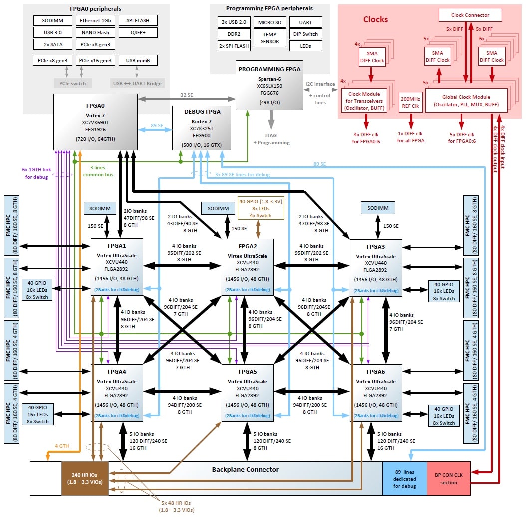
Aldec’s extra-large capacity board that features Xilinx UltraScale FPGA technology contains six XCVU440 logic modules and is the most advanced one-piece PCB prototyping board in the market. It is targeted to high-speed physical prototyping and emulation of complex ASIC and SoC designs. The board provides an estimated capacity of 158 Million gates and is easily extendable via backplane and daughtercard non-proprietary connectors (BPX & FMC). Three of six UltraScale FPGA modules are connected with six DDR4 SO-DIMM slots to support up to 48 GB of aggregated memory. Larger capacity of 633 Million gates can be achieved with four HES-US-2640 boards connected in the backplane board HES7BPX4. Highest I/O count packages of UltraScale devices and proper on-board traces routing assure reliable LVDS and GTH transfers up to the device inherent limits.
KINTEX ULTRASCALE+ FPGA Boards

HES-XCKU11P-DDR4
The HES-XCKU11P-DDR4 contains Kintex UltraScale+ XCKU11P FPGA belonging to the family of chips from Xilinx which provide the best price/performance/watt balance. Two QSFP-DD can provide high bandwidth and low-latency communication (up to 400 Gbps). Thanks to the SO-DIMM memory socket, there is available to connect external high-speed DDR4 memory module. FMC connector compliant with ANSI/VITA 57.1 standard provides easy extensibility and access to additional peripherals. These resources make the board very universal and can be used for many applications while maintaining a small size and affordable price.
VIRTEX-7 FPGA Boards
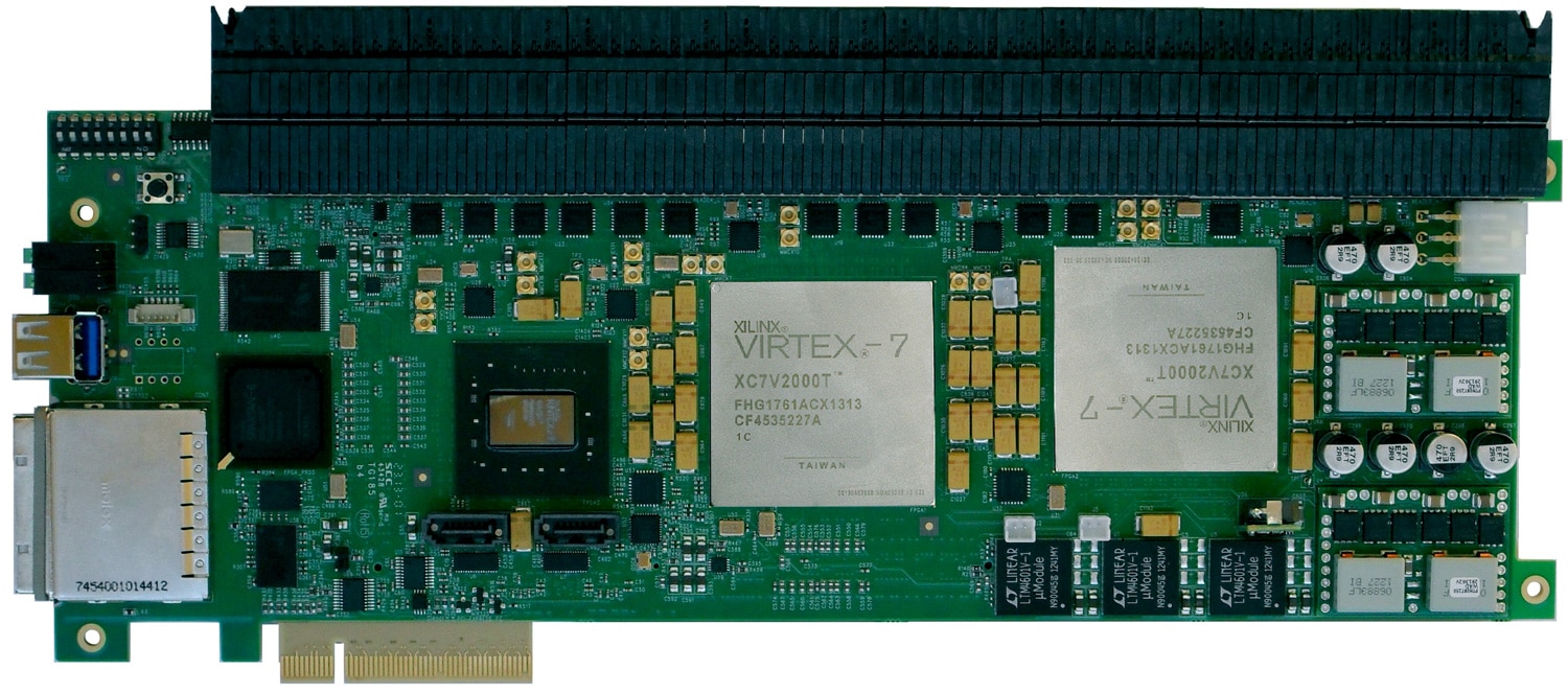
HES7XV4000BP/HES7XV1380BP Prototyping and Emulation Main Board
HES7XV4000BP and HES7XV1380BP are dual Virtex-7 FPGA prototyping and emulation boards for small-medium size ASIC designs or large FPGA designs. The board is available in two configurations with XC7V2000T or XC7V690T logic modules. The estimated capacity of the largest configuration is 24 Million ASIC gates and is easily extendable via backplane non-proprietary connector (BPX). Larger capacity of 96 Million gates can be achieved with four HES7XV4000BP boards connected in the backplane board HES7BPX4. There is one SO-DIMM slot for DDR3 memory connected to one of the Virtex-7 FPGA providing up to 8GB of external RAM to the emulated design. The highest quality PCB design with proper onboard traces routing assure reliable LVDS and GTX transfers up to the device inherent limits.
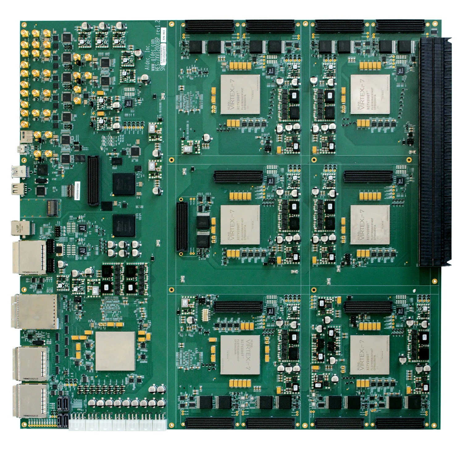
HES7XV12000BP Prototyping and Emulation Main Board
Aldec’s large capacity board that features Xilinx Virtex-7 FPGA technology contains six XC7V2000T logic modules and is the most advanced in the market one piece PCB prototyping board of Virtex-7 family. It is targeted to high-speed physical prototyping and emulation of complex ASIC and SoC designs. The board provides an estimated capacity of 72 Million gates and is easily extendable via backplane and daughter card non-proprietary connectors (BPX & FMC). Two of six Virtex-7 FPGA modules are connected with four DDR3 SO-DIMM slots to support up to 32 GB of aggregated memory. Larger capacity of 288 Million gates can be achieved with four HES7XV12000BP boards connected in the backplane board HES7BPX4. Highest I/O count packages of Virtex-7 devices and proper on-board traces routing assure reliable LVDS and GTX transfers up to the device inherent limits.
HES BACKPLANE Boards
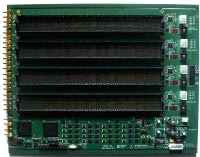
HES7BPX4 Backplane Board
HES7BPX4 is a backplane board used to build scalable hardware platforms for emulation and prototyping based on HES-US or HES-7 FPGA main boards. The largest configuration can supply up to 633 Million ASIC gates. The backplane is build of non-proprietary BPX connectors matching ones used on HES main boards to provide passive cross board I/O interconnections. Careful design of clock distribution tree assures flexibility and configurability from a host PC. There is a special backplane controller implemented in Spartan-6 FPGAs, that integrates JTAG chains and debug buses from all mainboards and provides a common programming port to all FPGA logic modules in the system.
Microchip FPGA Boards – Polarfire and Smartfusion SOC
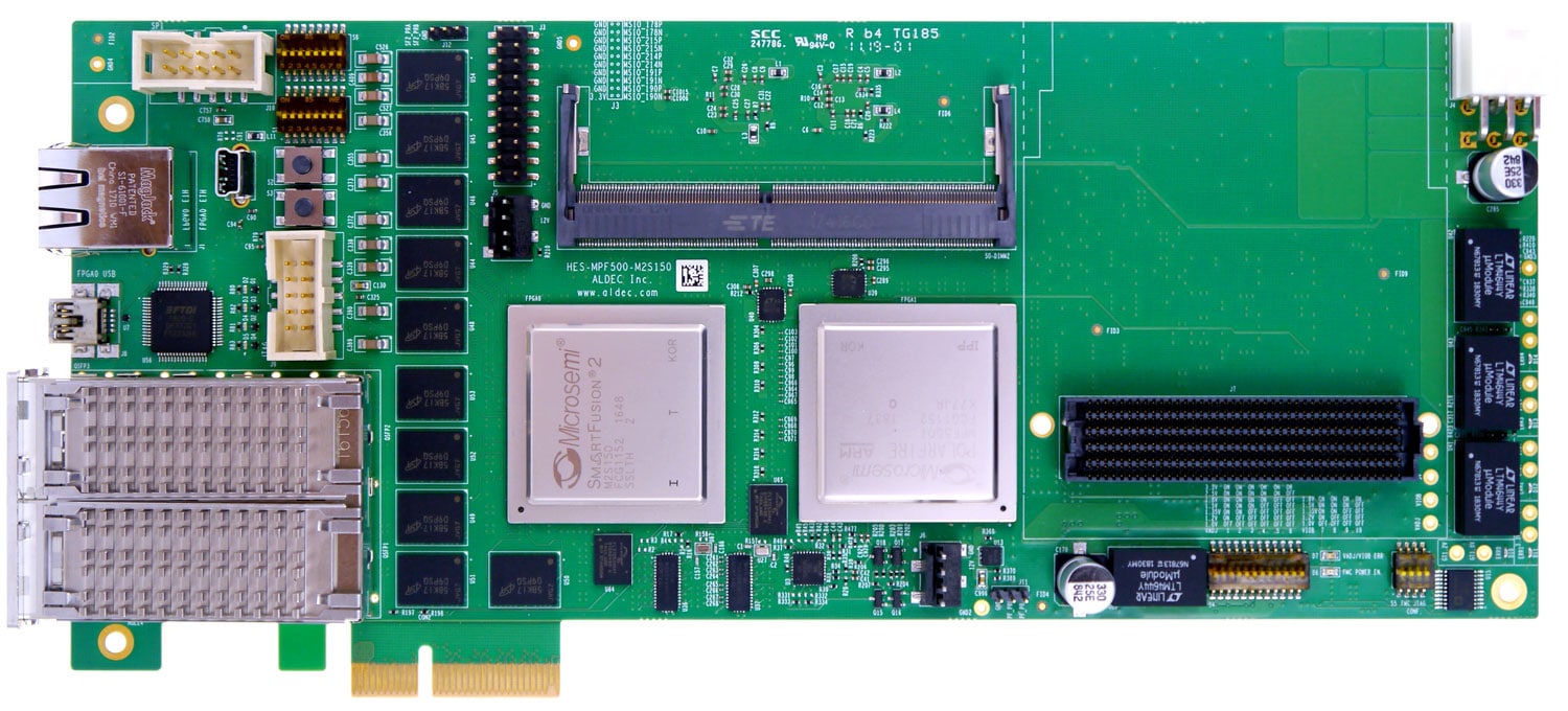
HES-MPF500-M2S150
The board HES-MPF500-M2S150 includes one Microchip PolarFire MPF500T FPGA logic module and one SmartFusion2 M2S150 SoC host module featuring ARM Cortex-M3. The board features a unique integration of a Microchip SmartFusion2 SoC FPGA and PolarFire FPGA.
Available onboard external memory resources include DDR4 SODIMM slot and 2x 8Gb DDR3 memory (16Gb total). The board contains PCIe x4 interface switchable between FPGA and SoC modules and two QSFP+ connectors for high-bandwidth low-latency communications. The FMC connector compliant with ANSI/VITA 57.1 standard provides easy extensibility, which Aldec FMC HPC connectors can use.

