Advancements in FPGA silicon, IPs, and tool flows have proven FPGAs to be the ideal solution for accelerating complex computational applications for solving science, engineering, and business problems. The inherent reprogrammability of FPGAs, deep pipelining structures, and massive parallel compute resources to favor the ever-evolving technology of High-Performance Computing (HPC) algorithms and applications in Genomics, Cryptography, etc Computer Vision, Neural Networks, Big Data, High-Frequency Trading. Moreover, with the same or even better results, FPGA can dramatically reduce power consumption and allow future upgrades and modifications.
Aldec has been providing FPGA design and verification tools for more than 30 years, gaining extensive knowledge of FPGA technology, industry standards, toolchains, hardware programming languages, and verification methods. Aldec’s goal is to share this experience in order to deploy the most energy-efficient HPC solution available today. Unlike other vendors that provide bare hardware, we will support your migration process to FPGA with development tools, reusable modules, and advisory services for the first time success. Aldec’s HPC turnkey solutions include three elements that are needed for accelerating and deploying HPC algorithms with scalable FPGA-based hardware.
- FPGA-based accelerators
- Reference designs and integration services
- HDL/RTL code design and simulation tools
FPGA Accelerators
Every customer’s needs are different and depend on the projects, therefore Aldec has developed a portfolio of FPGA accelerator boards to meet various expectations. Currently, Aldec provides several board configurations that can cope with the acceleration of the most demanding and sophisticated algorithms that fall in two main categories – Large Scale HPC and Embedded HPC.
Derived from the family ofHES prototyping boards, the FPGA accelerators were designed and optimized for large scale HPC applications To address the growing needs of embedded HPC, Aldec designed a particular family of compact TySOM boards that utilize Xilinx Zynq devices that integrate both ARM Cortex processors and FPGAs structures in one chip.
Fast Integration
Short bring-up time of algorithm mapped to FPGA and quick integration with the main application is what software developers need and request. Aldec understands HPC business and software development models as well as FPGA design processes, Therefore, they are able to provide integrated solutions that allow you to take advantage of FPGA technology and avoid hiring a team of hardware experts. The integration solutions include reusable software and hardware components such as HES Proto-AXI interface and advisory services to spread our knowledge and expertise. Aldec’s close cooperation with FPGA chip vendors and extensive knowledge of their toolchains for algorithm implementation will make your transition to FPGA efficient and problems.
Services & Reference Designs
Aldec believes in reusability and therefore offers customers numerous reference designs, both for large-scale HPC and embedded HPC platforms. Aldec’s customers do not have to start their projects from scratch but can reuse existing designs, which significantly reduces project time. If this is not enough, Aldec with its 30+ years of experience in FPGA/ASIC technology can offer and perform custom development services such as:
- Building a complete system optimized for your application
- Integration Ihrer Algorithmen in die FPGA-Hardware-Infrastruktur
- Conversion of an algorithm to the FPGA
FPGA design and simulation tools
Users looking for a complete FPGA development ecosystem will benefit from Aldec’s collaboration with its FPGA accelerator boards and RTL development/simulation tools such as Riviera-PRO – a powerful mixed-language simulator (VHDL/Verilog/SystemVerilog/SystemC) with Python testbench support for FPGAs.
Advantages
- Tailor-made hardware platforms – users can choose from large portfolio of FPGA boards for large scale and embedded HPC.
- Scalability – algorithm kernels replication is facilitated with support of multi-FPGA and multi-board configurations
- Quick integration & short bring-up with reusable components, processes and reference designs
- Complete development environment including RTL simulators and integration with FPGA vendor tools
Computer Vision
Computer vision requiring image processing algorithms is one of the most dynamically improving applications that benefits from FPGA processing power. Detecting moving objects is useful in monitoring, surveillance systems as well as in various industrial cases during automated production.
Aldec has developed a demo design that shows how FPGAs can be used to accelerate image processing algorithms that handle a large amount of input data and cope with high input and output bandwidths. The demo design provides RTL implementation of a motion detection algorithm called ViBe and uses the case of detecting moving objects in a video data stream. The example also demonstrates that algorithm execution can be further accelerated by replicating the ViBe function kernel and running video processing in parallel threads utilizing efficient resources of large FPGA, Xilinx Virtex UltraScale XCUS440. It also demonstrates how to connect an algorithm kernel running in FPGA with PC Host Workstation through Aldec HES Proto-AXI interface or access on-board DDR.
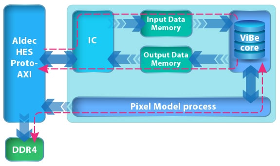
Most important functions
- Function: Detecting moving objects in video data stream
- Algorithm: Vibe Motion Detection
- Processing live data stream from USB camera connected to host
- Video resolution: Full-HD, 1920×1080
- Number of replicated algorithm kernels: 4
- Processing speed: 120 frames per second
Solution concept
- Accelerator board: HES-US-440
- Host workstation interface: HES Proto-AXI
- Host workstation interface: HES Proto-AXI
- RTL code of ViBe algorithm
- C++ code of the main program running on PC Host Workstation
Platform documentation
Encryption & Security
Encryption and decryption algorithms are used in many fields where the security of transferred data is required. It assures the safety of individuals, groups, and countries. New cryptographic algorithms such as AES and DES are more and more compute-intensive.
Security has become one of the critical factors in embedded designs, especially in the applications of Internet-of-Things (IoT) or Industry 4.0. Sensitive telemetric data are sent from the field of operation to the Cloud for further processing. The wireless channels are often used due to environmental conditions and mobility, but they are more vulnerable to hacking attacks. So, the gateway device which collects data and transfers them to the Cloud should provide encryption and decryption algorithms.
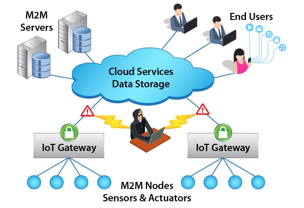
FPGA integrated with the processing system as in Xilinx Zynq devices is a convenient platform to implement hardware accelerator of cryptographic algorithm which can be additionally customized (thus safer) and won’t overload embedded processor free to execute other programs simultaneously. Based on Zynq devices, Aldec provides the TySOM product line for embedded applications, including Embedded HPC.
To demonstrate the power of FPGA in the cryptography and IoT application we have created a demo design of a gateway device with the AES encryption algorithm implemented in FPGA and used to secure the data transferred outside via the WiFi interface. Data collected from various sensors and aggregated by the ARM Processing System are then AES-encrypted before being exposed in the WiFi interface. The receiving device can then decode data with the private key stored locally. This demo can be used as a reference design and the base for further customizations and implementations.
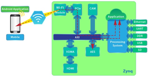
Most important functions
- Reference design of IoT Gateway with data encryption
- Hardware implementation of AES encryption algorithm
- Main application running in embedded Linux environment
- Demonstrates use of ARM Processing System with FPGA for acceleration in one chip
- Provides options to connect edge devices (sensors & actuators) communicating with different standards: Bluetooth, Z-Wave, ZigBee, USB
Solution concept
- Hardware platform: TySOM-1 – board with Xilinx Zynq-7000 device
- AES accelerator RTL code
- Gateway embedded design reference implementation – hardware and software
- Embedded Linux, Debian linaro-jessie-alip
- Platform documentation
Genome Alignment
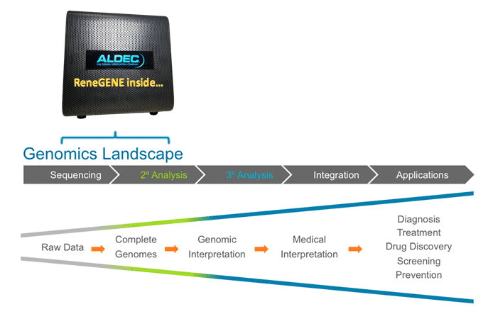
Scientific researches at many fields need computational power sometimes even more than industrial applications To demonstrate the power of FPGA, Aldec and the Indian Institute of Science faculty enterprise, ReneLife, implemented the algorithm of ReneGENE for accurate genome alignment on Aldec’s HES-HPC FPGA-based accelerator.
ReneGENE offered on HES-HPC as AccuRA, for accurate, and ultra-fast big data mapping and alignment of DNA short-reads from the Next Generation Sequencing (NGS) platforms, with full coverage of the genome (million to billion bases long), including repeat regions. The technology, devoid of heuristics can precisely align the DNA reads against a reference genome at a single nucleotide resolution. As genomics permeates the entire landscape of biology, including biomedicine and therapeutics, ReneGENE creates a genomic highway that significantly contributes to reducing the time from sample to information without compromising on accuracy, critical for lifesaving medicare applications, biotechnology product development, and forensics.
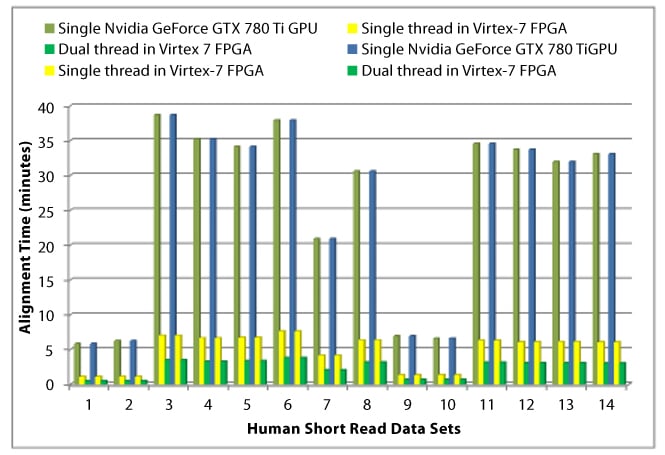
- Aldec HES-HPC is ~10x faster than GMAccS, the single GPU OpenCL
- Aldec HES-HPC is ~26x faster than CUSHAW, the open source single GPU CUDA
- GMAccS demonstrates a speedup over 150x compared to the standard heuristic aligners like BFAST, so AccuRA is several orders faster than the competitors
- HES-HPC has more available FPGA resource for more hardware kernels, possible to put up to 6 kernels in one FPGA
Most important functions
- Fully streaming, multithreaded, parallel dynamic programming in hardware eliminates memory bottleneck and storage issues
- Reduces computing and I/O burden on the host significantly
- Achieves short read mapping in minimum deterministic time
- Highly accurate and precise SRM solution
- Fastest genome aligner in the market
- Scalable at multiple levels of design granularity, massively parallel solution
- Scalable in data size, ranging from genome sizes of millions to billions
- ReneGENE AccuRA most cost-effective solution. The customer will incur less than one percent of his monthly expenditures for ReneLife-Aldec solution compared to conventional cluster, and also save time due to accelerated performance.
- The results of the alignment from ReneGENE are available in a standard format, called.SAM or its equivalent binary known as.BAM, can be processed by the downstream analysis tools in any lab across the globe.
- End-users include NGS OEMs Large research groups Medical research groups and hospitals Small research groups and diagnostics labs forensics Individuals like clinicians
Solution concept
- ReneGENE software application
- AccuRA system running on HES-HPC
High Frequency Trading
The popularity and value of FPGAs for High-Frequency Trading (HFT) systems have increased over the last five years – and the primary reason is latency. HFT firms must utilize the latest technologies in order to achieve close-to-zero latency to remain competitive – whoever has the fastest system wins.
FPGAs consists of millions of logic gates that can process data in parallel as opposed to software that execute data sequentially. Thus, FPGAs can provide deep sub-microsecond latency compared to several microseconds via software. FPGAs include thousands of DSP blocks that can execute mathematical computations in parallel, and FPGAs are also re-programmable, enabling flexible systems that can be optimized even in the field.
With Aldec’s 30+expertise in FPGA/ASIC prototyping and acceleration, we provide FPGA accelerators with PCIe and QSFP interfaces and are compatible with 1U (or larger) trading systems for time-sensitive trading strategies such as Market Making, Statistical Arbitrage, and Algorithmic Trading.
Achieving Low Latency
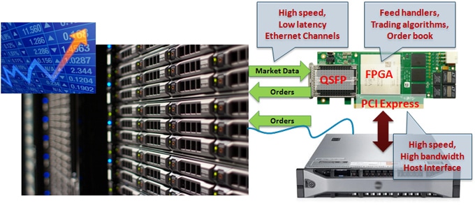
Low latency which is the paramount requirement was achieved by using the newest generation Xilinx FPGA – Virtex™ UltraScale+ and connecting all critical interfaces like Ethernet/QSFP and PCI Express directly to the FPGA. Market data feeds captured directly from the network interface (QSFP) are immediately processed inside the FPGA fabric that can accommodate hundreds of parallel processors specialized for a given task. The second QSFP link can be used to trigger buy, sell or cancel orders based on the results of the algorithm running entirely in FPGA. Alternatively, pre-processed data can be moved to the host workstation via the PCIe interface for analysis in existing software. The pipelining features of FPGA allow for all the interfaces to operate in parallel.
Re-configuration on-the-fly
The FPGA can be re-configured on the fly without the need of shutting down the entire system which greatly increases the flexibility of such configuration and facilitates quick reaction to dynamically changing trading conditions. The new FPGA accelerators are compatible with 1U and larger trading systems for time-sensitive trading strategies.
Develop and debug FPGA designs
Customers looking for a complete FPGA development eco-system will benefit from cooperation with Aldec with its FPGA accelerator boards and RTL development/simulation tools such as Riviera-PRO – a high performance mixed-language (VHDL/Verilog/SystemVerilog/SystemC) simulator with Python testbench support for FPGAs.
Integrate with IP partners providing IP-cores critical for implementing market data feed handlers and other blocks of the trading system.
Most important functions
- Fast processing in newest Xilinx UltraScale+ FPGA
- Higher level speed-grade (-2) of used FPGA
- Low latency interfaces QSFP28
- High bandwidth host interface PCI Express 16x, gen3
Fast QDR-II memories - Low profile boards (can be used in 1U rack servers)
- Hot-reconfiguration (FPGA change without power down & PCIe link active)
- Solution vendor with FPGA designing know-how
Solution concept
- FPGA board, low profile, PCIe, low latency interfaces, 1U-rack server supported
- Riviera-PRO High-Performance Simulator for algorithm development in HDL
- IP-partners for low latency ethernet
- Reference and diagnostic designs with QSFP and PCIe interfaces and QDR-II memory controller
Large Scale HPC
FPGA acceleration has been a key enabler to solve today’s bleeding edge computational problems. Neural Networks deep learning, data mining, cloud computing or scientific research are just a few fields where traditional servers lack computational power despite consuming a lot of energy. Recent, tremendous advances in FPGA technology has opened the door for its use in HPC applications.
Aldec’s scalable, FPGA accelerators are ideal for large scale HPC applications Today’s generation of FPGA accelerator boards features low power, Xilinx® Ultrascale™ FPGAs providing outstanding computational capabilities with power efficiency not achievable with the GPU-based accelerators.
FPGA Accelerators
HES-XCVU9P-QDR – low profile form factor board with PCIe x16 that can be installed directly inside servers used in data centers. On this board FPGA is mated with high bandwidth QDR-II+ memories provide high throughput for algorithm acceleration.
HES-XCVU9P-ZU7EV – board with separate host interface chip Xilinx Zynq UltraScale+ XCZU7 and another FPGA Xilinx UltraScale+ XCVU9P designated entirely for user’s application. Its logic resources contain many DSP blocks (6840), making it ideal for DSP and computer vision applications.
HES-US-440 – stand-alone board with external PCIe x8 cable connection contains the most potent Xilinx Virtex Ultrascale device with an unprecedented capacity of 5.5 million logic cells, DDR4 memory up to 64GB in two modules, and fast RLDRAM. It is dedicated to accelerating very complex algorithms or those which can benefit from a large number of replicated instances of the algorithm kernel.
HES-XCKU11P-DDR4 – low profile form factor board with PCIe x16 that can be installed directly inside servers used for HPC/HFT. Includes Kintex UltraScale+ which belongs to the best price/performance/watt balance FPGA family. Two QSFP-DD can provide high bandwidth and low-latency communication (up to 400 Gbps).
| HES-XCVU9P-QDR | HES-XCVU9P-ZU7EV | HES-US-440 | HES-XCKU11P-DDR4 | |
|---|---|---|---|---|
| Logic Cells | 2.5 Million | 2.5 Million | 5.5 Million | 653,000 |
| DSP Blocks | 6840 | 6840 | 2880 | 2,928 |
| On-chip RAM | 75.9 Mb BlockRAM 270 Mb UltraRAM | 75.9 Mb BlockRAM 270 Mb UltraRAM | 88.6 Mb BlockRAM | 21.1 Mb BlockRAM 22.5 Mb UltraRAM |
| Off-chip RAM | 432 Mb QDR-II (3x 144 Mb) Or in *-DDR version: 32 Gb DDR4 (2x 16Gb) 144 Mb QDR-II | 32GB DDR4 (2x 16GB) 2x 576Mb RLD3 | 32GB DDR4 (2x 16GB) 1152 Mb RLD3 (2x 576Mb) | SODIMM DDR4 Memory socket 512 Mb Flash Memory 2x 64 kb I2C EEPROM |
| Host Interface | PCI Express x16, gen3 | PCI Express x8, gen3 Zynq UltraScale+ XCZU7 | PCI Express x8, gen2 Zynq-7000, XC7Z100 | PCIe x16 gen3 endpoint or PCIe x8 gen4 2x QSFP-DD (total up to 400Gbps) |
Host Interface
Connecting the FPGA accelerator board with a host workstation via PCIe is not trivial and if done from ground up would require extensive knowledge of hardware design. Software developers need a ready-to-use hardware platform without low-level hardware integration implications. Understanding such a use model, Aldec provides HES Proto-AXI interface that hides low level PCI Express implementation details and saves your development time. The user receives HES Proto-AXI IP-core which is based on AMBA AXI standard and bridges accelerated algorithm kernels to the PCIe bus of host computer.
Aldec’s scalable, FPGA accelerators are ideal for large scale HPC applications Today’s generation of FPGA accelerator boards features low power, Xilinx® Ultrascale™ FPGAs providing outstanding computational capabilities with power efficiency not achievable with the GPU-based accelerators.
FPGA Accelerators
HES-XCVU9P-QDR – low profile form factor board with PCIe x16 that can be installed directly inside servers used in data centers. On this board FPGA is mated with high bandwidth QDR-II+ memories provide high throughput for algorithm acceleration.
HES-XCVU9P-ZU7EV – board with separate host interface chip Xilinx Zynq UltraScale+ XCZU7 and another FPGA Xilinx UltraScale+ XCVU9P designated entirely for user’s application. Its logic resources contain many DSP blocks (6840), making it ideal for DSP and computer vision applications.
HES-US-440 – stand-alone board with external PCIe x8 cable connection contains the most potent Xilinx Virtex Ultrascale device with an unprecedented capacity of 5.5 million logic cells, DDR4 memory up to 64GB in two modules, and fast RLDRAM. It is dedicated to accelerating very complex algorithms or those which can benefit from a large number of replicated instances of the algorithm kernel.
HES-XCKU11P-DDR4 – low profile form factor board with PCIe x16 that can be installed directly inside servers used for HPC/HFT. Includes Kintex UltraScale+ which belongs to the best price/performance/watt balance FPGA family. Two QSFP-DD can provide high bandwidth and low-latency communication (up to 400 Gbps).
Convert
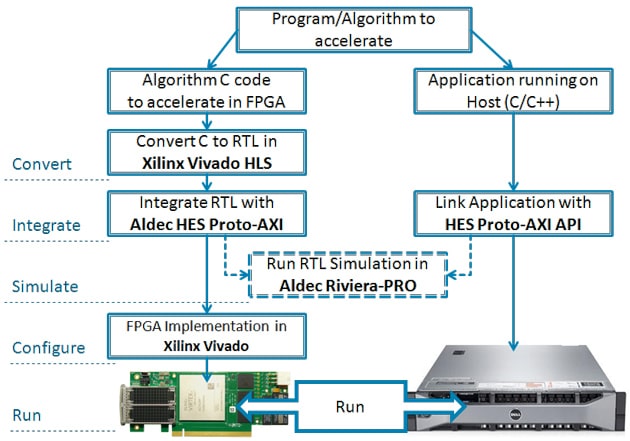
The program or algorithm to accelerate is partitioned in two parts – one designated for acceleration and the other that runs on the host. Such partitioning can be made based on the results of the profiling that indicate pieces of C code that are computationally intensive. Next, the Xilinx Vivado HLS tool is used to convert from C to Verilog or VHDL RTL code that is appropriate for further automatic processing (synthesis and implementation in FPGA). User should choose to include AMBA AXI interface in the RTL code which will be required for the next stage.
Integrate
Once the HDL code is available it needs to be integrated with Aldec HES Proto-AXI – that is connected to AMBA AXI ports. Using HDL editor tool such as one from Aldec’s Riviera-PRO is sufficient for this stage. Concurrently, the main application intended to run in the host computer is modified to replace calls of algorithm functions with their counterparts using the FPGA via HES Proto-AXI API.
Simulate
Before running the whole project with the FPGA accelerator board, you can verify it against any integration/connectivity mistakes by using Aldec’s high-performance Riviera-PRO simulator and the HES Proto-AXI simulation model included in the Large Scale HPC solution.
Configure
The last stage is automatic Synthesis and Implementation using the Xilinx Vivado environment that generates FPGA bitstream and configuration files for your primary application.
Run
Aldec provides run-time environment that makes FPGA accelerator boards usage straightforward. The PCI Express device driver is installed and accelerator board housekeeping functions are included in the Proto-AXI API library linked with your program. When you launch your main application on the host computer the FPGA is configured automatically, so any special knowledge of FPGA operation or programming is not required, thus it’s a very convenient environment for software developers.
Most important functions
- Choice of several FPGA accelerator board to match project requirements
- Scalability with multiple-board configurations support
- Supports hot-reconfiguration of FPGA
- Integrated with FPGA development and verification environment
Solution concept
- HES-HPC FPGA Accelerator board
- HES Proto-AXI host interface module and software stack
- AXI Bus Functional Model (BFM) for RTL simulation
- Riviera-PRO high performance HDL simulator
- Reference designs, technical documentation, tutorials and white papers
- Integration services
Embedded HPC
Recent years brought an outburst of embedded electronics, many of them containing very powerful microprocessor designs that outperform the capabilities of desktop computers available ten years ago. Smartphones are a common example, but there are hundreds of others. Computer vision, Automotive systems, UAV (drones), security cameras, and network security are only a few categories where embedded electronics are present.
The Embedded HPC is the response for the growing appetite for computational power in embedded applications. These kind of applications require CPU and FPGA to be on the same board and ideally in the same chip. For this reason, Aldec’s TySOM boards were based on the Xilinx Zynq family of MPSoC and chipsets that integrate ARM Programmable System and FPGA.
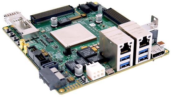
TySOM-3A-ZU19EG is a compact SoC prototyping board featuring Zynq® UltraScale+™ MPSoC device which provides 64-bit processor scalability while combining real-time control with soft and hard engines for SoC prototyping solution, IP verification, graphics, video, packet processing, and early software development Der Hauptvorteil des Xilinx Zynq Ultrascale+ ZU19EG-FFVB1517 MPSoC gegenüber anderen Zynq MPSoC-Bausteinen besteht darin, dass er das größte FPGA der Zynq® UltraScale+™ MPSoC-Familie mit über einer Million Logikzellen enthält. The main advantage of Xilinx Zynq Ultrascale+ ZU19EG-FFVB1517 MPSoC over other Zynq MPSoC devices is that it carries the largest FPGA in the Zynq® UltraScale+™ MPSoC family with over a million logic cells. It includes a quad-core ARM® Cortex-A53 platform running up to 1.5GHz. Combined with dual-core Cortex-R5 real-time processors, a Mali-400 MP2 graphics processing unit, and 16nm FinFET+ 1,143K logic cells in the programmable logic. This prototyping board contains 8GB DDR4 Memory for the Programmable Logic (PL) and also 8GB DDR4 SODIMM Memory for the Processing System (PS). This board includes 2 Gb NAND Memory and supports up to 32GB of SSD storage in a Micro-SD card. It also features a 512Mb QSPI Flash Memory. Communication and networking is enabled by ×2 Gigabit Ethernet, Wi-Fi & Bluetooth, CAN, Pmod, 4× USB 3.0, USB to UART Bridge, USB 2.0 OTG, JTAG USB, SATA, QSFP+, and PCIe x1 GEN3/4 connectors. Multimedia interfaces are provided using DisplayPort, HDMI IN/OUT. To expand the peripherals, 2× FMC VITA 57.1-2010 compliant are provided on the board. Thus, additional devices can be connected as FMC Daughter Cards that are provided by Aldec.
TySOM-3-ZU7 – accelerator board based on Zynq UltraScale+ ZU7EV containing FPGA with Quad-core ARM Cortex-A53 general-purpose processor, ARM Cortex-R5 real-time processor, ARM Mali-400 graphics processor, and H.264/H.265 video codec. Video-Codec. The embedded FPGA can be used to accelerate the most critical functions of the embedded application or to implement the glue logic for external device interfaces. ZU7EV’s heterogeneous architecture is a powerful platform for various applications such as neural networks, encryption, or image and video processing.
TySOM-2 – Accelerator card based on the Zynq-7000 XC7Z100 with a dual-core ARM Cortex-A9 general-purpose processor in one chip and the largest FPGA in the Zynq-7000 family. The large number of DSP blocks (2020) makes it perfect for embedded vision applications.
Design Automation
To facilitate the design of embedded HPC applications, Aldec offers TySOM system platformsthat can be loaded into the Xilinx SDx tool. Then, in SDx C/C++ algorithm files are compiled and converted to RTL code appropriate for FPGA. Finally the RTL code is connected automatically to the selected system platform.
When all the compilation and implementation steps are done, running embedded application is as easy as uploading files generated from SDx to SD card and starting execution in TySOM board.
Reference Designs and Services
For a quick ramp-up Aldec provides several reference designs demonstrating the use of different peripherals and programmable logic (FPGA) to accelerate application algorithms and working implementation of embedded Linux. If you recognize the benefits of FPGA-powered embedded HPC, but your organization lacks hardware design “know-how,” Aldec’s custom engineering services can bridge this gap. Our long experience in FPGA hardware design and verification can be effectively used to quickly build a complete system or integrate your algorithms with reference designs that are available out of the box.
Most important functions
- Portfolio of TySOM boards for various requirements
- Compatible with complementary FMC daughterboards
- Complete design and verification environment
- Tight integration with Xilinx SDx and Vivado software
- High quality and solid hardware
Solution concept
- Aldec TySOM-Platine
- TySOM reference designs in the package
- Riviera-PRO HDL Simulator(optional)
- Technical documentation, tutorials and white papers
- SDx Hardware Platform Package (Board Support Package – BSP)
- Custom development for RTL Porting Services
